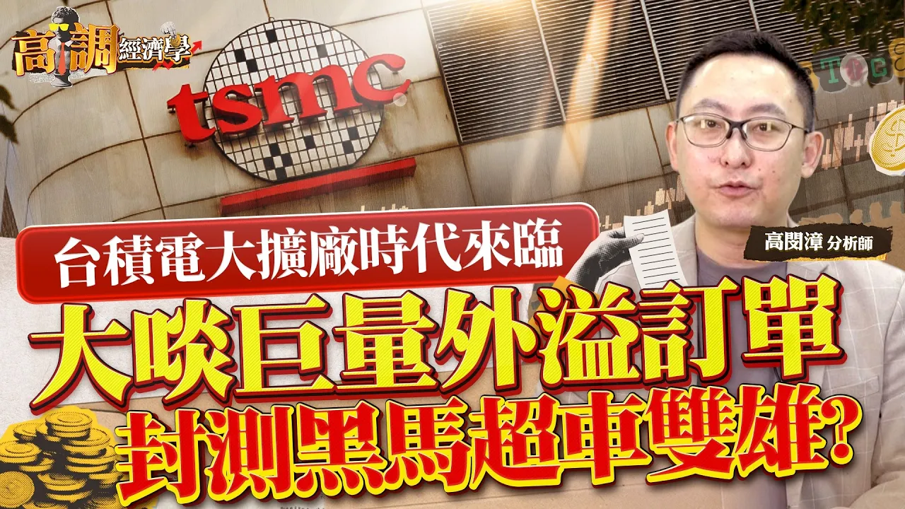
⚡ Engineering Insight
The burgeoning demand for AI and High-Performance Computing (HPC) has unveiled a critical bottleneck in the semiconductor supply chain: advanced packaging capacity. While TSMC leads with its CoWoS (Chip-on-Wafer-on-Substrate) technology, a 2.5D integration solution essential for integrating high-bandwidth memory (HBM) with logic dies, its current expansion efforts are struggling to keep pace with the exponential growth in AI accelerator orders. This capacity crunch, particularly acute for CoWoS, is forcing a strategic pivot across the industry. Significant "spillover" orders for advanced packaging and testing are now cascading to Outsourced Semiconductor Assembly and Test (OSAT) providers, transforming their operational landscape and elevating their role from traditional backend services to critical enablers of next-generation AI architectures. This dynamic highlights the increasing complexity of heterogeneous integration and the distributed nature of the advanced semiconductor manufacturing ecosystem.
🛠️ Key Specs & Data
- CoWoS Technology: TSMC's proprietary 2.5D/3D advanced packaging solution, integrating logic dies (e.g., GPUs, AI ASICs) with HBM stacks on a silicon interposer, then mounted on a substrate. Critical for high-throughput, low-latency AI compute.
- Capacity Shortfall: Despite TSMC's aggressive capital expenditure on advanced packaging (including CoWoS, InFO_PoP, CoPoS, 3DIC), current output remains insufficient to meet the surging demand from key AI players like NVIDIA, Amazon, and Google. Lead times for CoWoS packaging are reportedly extending beyond industry norms.
- OSAT Beneficiaries:
- ASE Technology Holding (ASEH): As the largest OSAT, ASEH is strategically positioned to capture a significant portion of the advanced packaging spillover. Its capabilities in heterogeneous integration, including advanced flip-chip BGA (FCBGA) and System-in-Package (SiP) solutions, make it a primary candidate for complementary packaging work or specific module integration beyond TSMC's direct CoWoS capacity. The company's scale and established client relationships provide a robust platform for scaling.
- Kyocera (京元電子): Specialized in IC testing, Kyocera is a key player in the test phase for high-performance chips, including those destined for AI applications. Its reported penetration into NVIDIA's supply chain for final testing (FT) and burn-in testing (BIT) indicates its critical role in validating the quality and reliability of AI accelerators. The increasing complexity of these chips demands sophisticated test methodologies and equipment.
- Ardentec (欣銓): Focusing on wafer sort (WS) and final test, Ardentec is also expanding its footprint in the AI sector, alongside a recovery in automotive IC testing. Its strategic investments in high-performance testing platforms position it as a "dark horse" for testing complex ASICs and specialized HPC components, complementing the broader advanced packaging ecosystem.
- AI Accelerators: Primarily GPUs and custom ASICs, characterized by large die sizes, high power dissipation, and critical reliance on HBM integration, directly driving the demand for CoWoS and subsequent advanced testing.
⚖️ Pros & Cons
Pros:
- Diversification of Advanced Packaging Ecosystem: The spillover benefits OSATs, fostering a more distributed and resilient supply chain for advanced packaging, reducing single-vendor dependency (TSMC) for certain integration steps.
- Accelerated Innovation in OSATs: Increased demand for sophisticated packaging and testing pushes OSATs to invest in advanced technologies, R&D, and equipment, potentially leading to new, complementary integration solutions beyond TSAT's primary offerings.
- Enablement of AI Growth: By absorbing excess demand, OSATs prevent the advanced packaging bottleneck from severely impeding the deployment and scaling of critical AI infrastructure, thus sustaining the momentum of AI innovation.
- Enhanced OSAT Revenue and Market Position: For the specific OSATs capable of meeting these demanding requirements, it signifies a significant uplift in revenue, profitability, and strategic importance within the semiconductor value chain.
Cons:
- Continued Core CoWoS Dependency: While OSATs can handle spillover, the fundamental CoWoS integration remains predominantly with TSMC. OSATs primarily augment the ecosystem with complementary packaging (e.g., subsequent module integration, advanced substrate assembly) and critical testing, rather than fully replicating CoWoS.
- Quality and Yield Management Challenges: Distributing advanced packaging and testing across multiple vendors introduces complexities in maintaining consistent quality, yield, and intellectual property protection across the supply chain, requiring stringent vendor qualification and coordination.
- Significant Capital Expenditure for OSATs: Meeting advanced packaging and testing demands necessitates substantial investments in high-end equipment, cleanroom facilities, and specialized engineering talent, which can be a barrier for smaller or less financially robust OSATs.
- Interoperability and Standardization: Ensuring seamless interoperability between components packaged by different vendors, especially in complex 3D integration schemes, poses ongoing engineering challenges that require industry-wide standardization efforts.
Conclusion
The current CoWoS capacity shortfall at TSMC, while a short-term constraint for AI accelerator production, is a clear long-term catalyst for the OSAT industry. It underscores the undeniable shift towards heterogeneous integration and the critical role of advanced packaging and testing in unlocking the full potential of AI and HPC. OSAT leaders like ASEH, Kyocera, and Ardentec are strategically positioned to capitalize on this surge, transforming from traditional backend service providers to indispensable partners in the advanced semiconductor ecosystem. Their ability to scale, innovate, and maintain rigorous quality control will be paramount. This distributed model of advanced manufacturing, where specialized OSATs augment the capabilities of leading foundries, is not merely a stop-gap measure but a fundamental evolution towards a more robust, diversified, and technologically sophisticated supply chain essential for the future of AI.
Source: 台積電先進封裝全面擴產,CoWoS仍然供不應求,巨量的外溢訂單,將讓哪家OSAT大廠成為AI產業最大的長線受惠者?《#高調經濟學 EP.12》| #高閔漳

