🚀 Insight
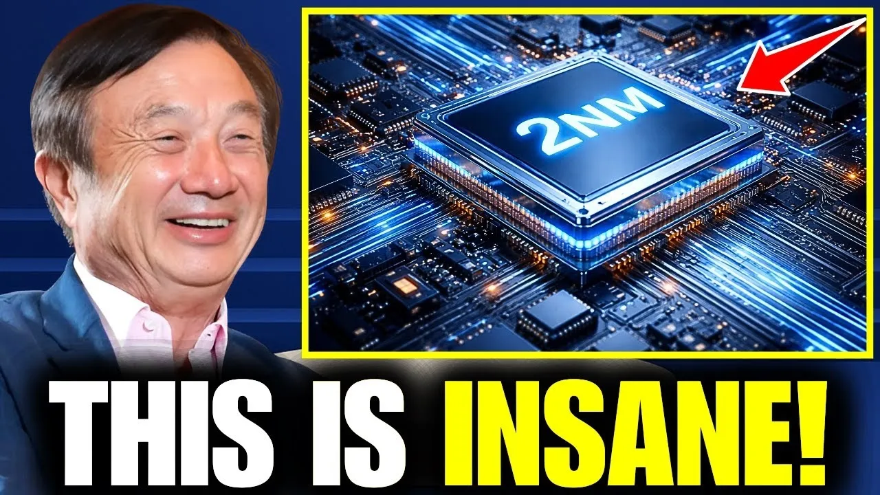
On December 6, 2025, the semiconductor world shifted. Huawei has officially filed a technical patent for 2-nanometer (2nm) chip manufacturing, a feat that global experts deemed physically impossible without ASML’s $150 million EUV (Extreme Ultraviolet) lithography machines. By leveraging Self-Aligned Quadruple Patterning (SAQP) and Deep Ultraviolet (DUV) light, Huawei isn't just circumventing Western sanctions—they are rewriting the rules of silicon physics. While TSMC and Intel rely on the 13.5nm wavelength of EUV, Huawei is effectively "drawing a line thinner than DNA" using 193nm DUV light. It is a desperate, expensive, and brilliant maneuver that signals the end of the "EUV-or-nothing" era.
⚙️ Deep Dive
The technical blueprint, titled "Metal Integration Method for Manufacturing Integrated Devices," reveals how Huawei plans to bridge the gap between 7nm and 2nm using older equipment. Here is the analytical breakdown of this high-stakes engineering:
- The SAQP Breakthrough: Instead of a single exposure with EUV, Huawei utilizes four passes with DUV machines. This involves creating "spacer" layers to incrementally narrow the features on the silicon.
- Exotic Metallurgy: To maintain conductivity at such microscopic scales, the patent specifies the use of Ruthenium, Cobalt, and Copper interconnects spaced at a staggering 21 nanometers.
- The Yield Crisis: This is the "Brutal Math." TSMC maintains a 90% yield for 7nm. For Huawei/SMIC to reach 2nm using DUV, yields are estimated at a crushing 10-15%. For every 10 chips produced, 9 are likely electronic waste.
- Subsidized Sovereignty: China’s $75 billion semiconductor fund is the "X-factor." Since Beijing prioritizes technological sovereignty over profit, they are willing to absorb 30% of manufacturing costs to ensure no foreign policy can shut down their domestic tech sector.
- Efficiency vs. Capability: While TSMC’s 2nm chips will be more cost-effective and energy-efficient, Huawei’s patent proves they can at least exist—a reality that forces the West to rethink the effectiveness of current lithography bans.
💡 Verdict
Is TSMC in "serious trouble"? Not in the short term. With a 30-year head start and a 90% yield advantage, TSMC remains the undisputed king of efficiency and volume. However, the "technological wall" built around China has officially cracked. Huawei has a history of making the "impossible" possible: they hit 7nm in 2023 and 5nm-level performance in 2024. While a patent is not a product, and mass production is likely 3-5 years away, the message is clear: Innovation under pressure is China's new superpower. The global chip war is no longer about who has the best machines, but who can innovate the most radical workarounds.
Source: 3 MIN AGO: Huawei Drops 2nm SHOCK Announcement..... TSMC in SERIOUS TROUBLE!
🛠️ Dive Deeper into the Engineering Core
👉 Click here to read the full technical breakdown on our Community Forum!

